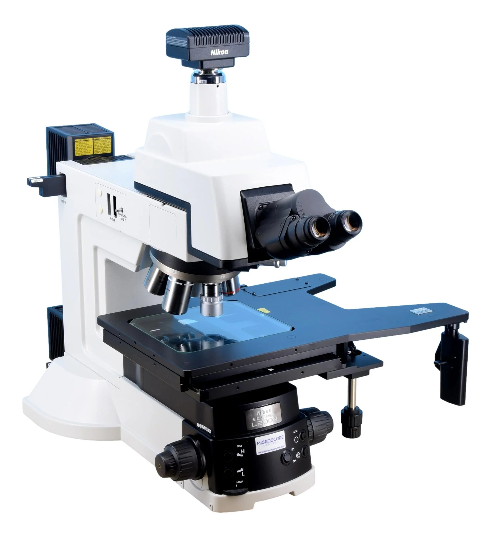
Nikon’s ECLIPSE L200ND, L200NA series of semiconductor microscopes are ideal for inspecting integrated circuits (ICs), flat panel displays, large scale integration (LSI) electronic devices and many other applications.
All cameras in Nikon’s Digital Sight range can capture images of a specimen and transmit them to the NIS-Elements image processing software, along with microscope data on the objective lens used, magnification setting and light intensity.
Reflected light: brightfield, darkfield, polarized (POL), differential interference contrast (DIC), epifluorescence and dual beam interferometry. Transmitted light illumination: brightfield, darkfield, polarization, differential interference contrast and phase contrast.
Nikon’s innovative design enables sharp, high-contrast optical contrast imaging techniques in brightfield, darkfield, polarization (POL), differential interference contrast (DIC) and two-wave interferometry.
Intelligent digital communication
The microscope detects and controls the objective lens used, light intensity, incident illumination and aperture via a USB connection to Nikon’s NIS-Elements software.
Ergonomic design concept
Thanks to the optimal positioning of the operator controls and the variable angle of the eyepiece, work is carried out without fatigue. The upright, erect image allows optimal observation of raw materials, semiconductors and industrial components.

Reviews
There are no reviews yet.